Hardware behind caches and main memory
Fetching value by address
For getting the value from main memory, the CPU has to go through the north bridge. The memory controller of RAM is attached to the north bridge. Another way to solve this is having the memory controller attached to the CPU, but this creates an overhead when one CPU wants to read the memory connected to another CPU.
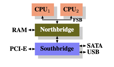
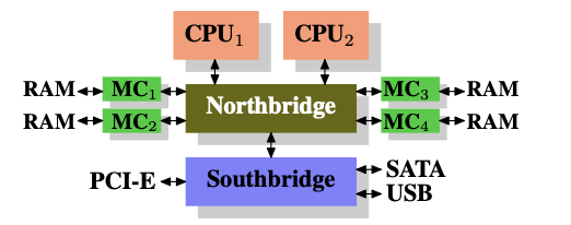
A modern RAM can have up to 4 GB of data, which is around 2^40 bits. For getting value from a bit, we have to access it directly. Having CPU connected directly to these transistor is not viable.
Instead, We have a multiplexer. Let’s say the address is of 32 bits. The multiplexer will input 32 address lines and will have an output of 2 to the power of 32 different individual lines to each transistor. This way, the CPU can have fewer lines, but still the memory will need a lot of infrastructure for these lines to access these individual values, which is again not feasible as we grow, as RAM grows in size.
Next, we divide these address lines by row and column, so 16 bits for the row axis and 16 bits for the column axis. This comes around 2^16, which is 65,000 lines, which is a lot better compared to 2 to the power of 32 individual lines.
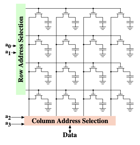
Having 32 pins just to address memory on CPU is very expensive. CPU has limited pins, and it is optimal to use them wisely. So what we have is the row and xs, and the column axis bits are signed separately over the same 16 pins. RSA signal, which is row access signal, is maintained for some time, and then when the column access signal comes, we are able to address a specific unit which holds the required value.
SRAM and DRAM
There are two types of RAM available in the market: SRAM and DRAM, S and D standing for Static and Dynamic. SRAM is a power-hungry six-transistor system where VDD has to be applied constantly to maintain the state, though since it doesn’t use a capacitor, setting and reading a value from it is instantaneous. As with DRAM, the system is one transistor, one capacitor. The capacitor discharges every 64 ms, and it has to be recharged again. It is less power hungry because there’s no need for constant voltage. It has two lines: AL and DL, which are access line and data line.
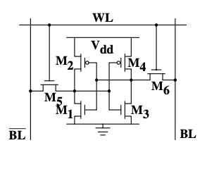
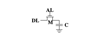
Main memory is mainly comprised of DRAM because it is less power hungry and can fit more transistors or bits on a small hardware. When in DRAM, it’s like synchronous; you will hear SDRAM term using used.
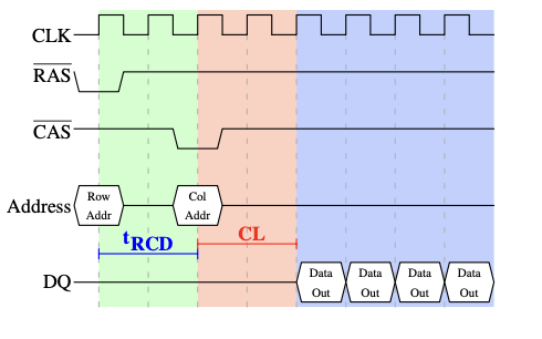
There is some required delay between row address and column address signal before the data can be sent out.
Note: With all this preparation to get to the data it would be wasteful to only transfer one data word. This is why DRAM modules allow the memory controller to specify how much data is to be transmitted. Often the choice is between 2, 4, or 8 words. This allows filling entire lines in the caches without a new RAS/CAS sequence
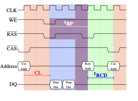
If you want to switch to a new row, it takes tRP, which is time to precharge a row before a new row can be selected. So from the large data transfer awakening, it takes TBR, then TRDC, and then RC before new transfer can be which is 7 clock cycles, and only 2 data cycles. so only 2/7 clock frequency is actual data speed of RAM. 2/7 is in case of new row selection , it is possible to keep same row signal active and get different row which will reduce it to 2/4.
Let’s say the front side bus, which connects the north bridge and CPU, has a speed of 100 MHz, and we are transferring 64 bits, which is 2 words, per 2/7 cycles. 6400*2/7 which is 1.8 Gbits per second.
In modern days, we are not transferring once per clock cycle. We have infra to double pump, which is transfer on up flink and down flink of the cp cycle.
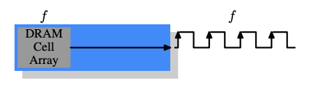
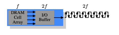
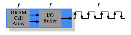
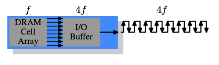
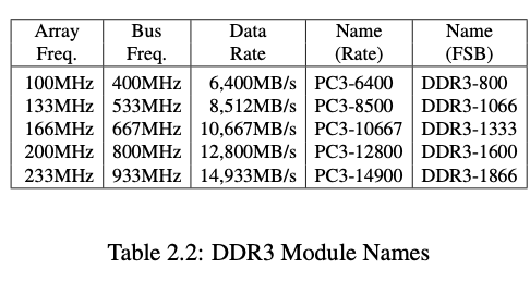
The DRAM unit has a frequency of 100 MHz, but it has 4F I/O buffer which makes quad pumped. And data is sent on both up/down flank, i.e. effective f is of 800MHz. 8 bytes per access will result in max transfer speed of 6400 MB/s.
CPU Caches
Modern CPU has a multi-layered cache. These caches are like the RAM unit; they are a lot faster than the main memory. The data is loaded into cache in the form of cache lines, which are 64 to 128 bytes. DRAM allows us to fetch 2 to 4 words (8/16 bytes) per data access, which means 8 to 16 transfer are needed to fill cache line. The cache can be divided into two caches: data cache and instruction cache.
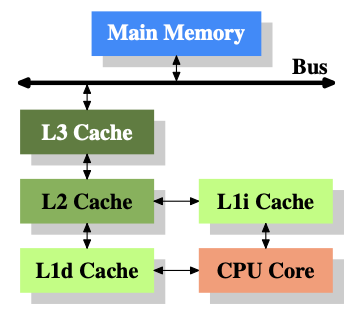
These caches, are separate because the properties of the data and instruction segments are different.
Modern computers can have multiple CPUs and multiple cores for CPUs. Each CPU has its own L1, L2, L3. The cores will have separate L1s but shared L2s and L3s. Each core can have multiple threads inside of it. Each thread uses the same core resources except for the registers. Threads share l1 cache.
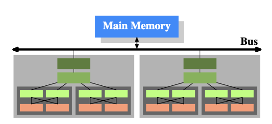
Instruction Cache Instructions are generated by the compiler to be optimized for branch prediction, while preferring temporal(data use now can be used later too) and spatial(next access will be Near by current access) locality. Modern CPU has 22-30 cycles in the pipeline where instructions are handled in different stages of fetching, decoding, and executing. This allows the CPU to not waste resources by being idle. Once the instructions have been decoded, the instruction cache L1I stores them. (it is also called trace cache, bcz of storing decoded instructions). Not much improvement can be done on the instruction cache site by application programmers.
Data cache Speed of the code execution depends on how the data is structured. If we have spatial and temporal locality, the execution will be a lot faster because of low miss cache factor.
MESI protocol
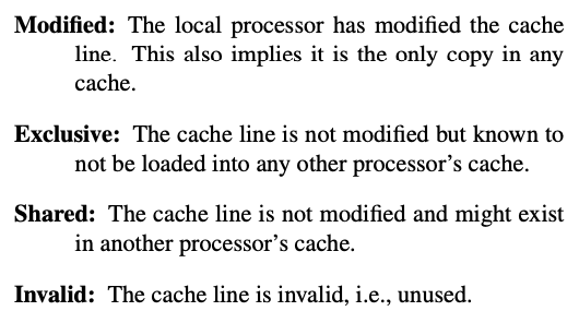
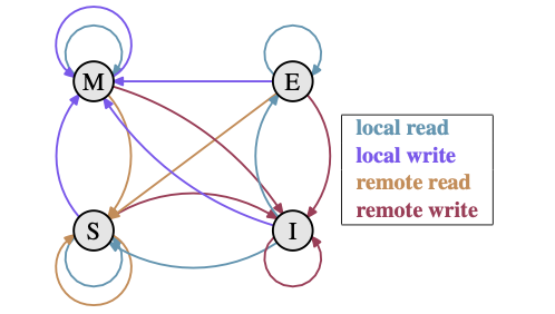
It’s a cache coherency protocol hardware protocol. It states how data read and write for memory cache lines that can be shared or exclusive is handled.
Local Read or Local Write are operations performed by core to the cache lines in its own cache. Remote operations are to the value that is present in cache of other core. The element caches of a single CPU are connected by an internal bus.
Links
https://www.youtube.com/watch?v=r_ZE1XVT8Ao&t=493s cache coherency mesi protocol